

Gan On Si Epi Wafers Market Growth: Accelerating the Power Electronics Revolution
The Gan On Si Epi Wafers Market Growth is a direct response to the global push for electrification and digitalization. As traditional silicon reaches its physical limits, industries are desperately seeking alternatives that can handle more power in smaller footprints. This search has led to the widespread adoption of semiconductor epi wafers that utilize Gallium Nitride on Silicon substrates. The growth trajectory is further bolstered by the rise of power electronics wafers that enable higher switching frequencies, reducing the size of passive components like inductors and capacitors.
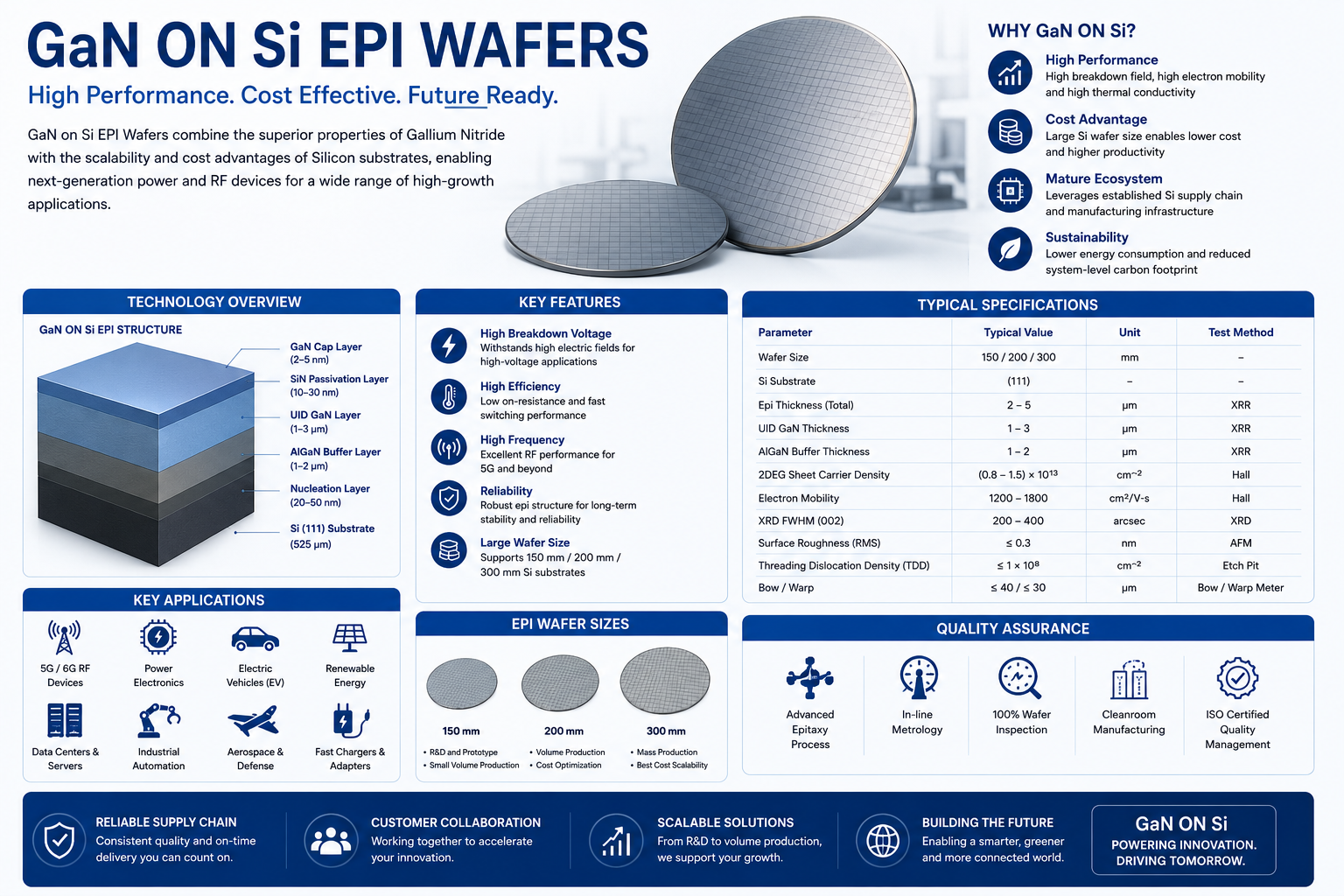
Market Overview and Introduction
Growth in this sector is not just incremental; it is exponential. The transition to GaN-on-Silicon technology is being hailed as the most significant event in power electronics since the introduction of the MOSFET. By growing GaN epitaxially on large-diameter silicon wafers, manufacturers can leverage existing CMOS-compatible foundries. This compatibility is the secret sauce behind the market’s rapid scaling, as it avoids the need for entirely new, multi-billion dollar manufacturing plants.
Key Growth Drivers
The primary engine of growth is the telecommunications industry. The rollout of 5G networks requires a vast number of small cells and base stations, all of which need high-efficiency power amplifiers. Furthermore, the renewable energy sector is increasingly turning to GaN to improve the efficiency of solar inverters. By reducing heat dissipation and energy loss, GaN-on-Si allows for smaller, more reliable inverters that can be easily installed in residential and commercial settings.
Consumer Behavior and E-commerce Influence
Modern consumers are increasingly "tech-literate" regarding the components in their devices. The "GaN" label has actually become a marketing tool for consumer electronics, with brands highlighting GaN technology to justify premium pricing for compact chargers. On the industrial side, e-commerce has streamlined the procurement of wide bandgap semiconductor materials. Engineers can now compare technical specifications and purchase wafers or pre-fabricated GaN-on-Si HEMTs through specialized online distributors, significantly shortening R&D cycles.
Regional Insights and Preferences
While China leads in sheer volume due to state-sponsored semiconductor initiatives, Japan and Europe are the leaders in high-quality epitaxial growth and device design. European automotive manufacturers are particularly keen on GaN-on-Si for auxiliary power systems in vehicles. In North America, the focus is largely on aerospace and defense applications, where the high-frequency capabilities of GaN are used in advanced radar systems and satellite communications.
Technological Innovations and Emerging Trends
One of the most exciting trends is the move toward "Vertical GaN" structures, which could potentially allow for even higher voltage ratings, pushing the technology into the territory currently dominated by Silicon Carbide. Additionally, the development of "Enhancement-mode" (E-mode) GaN transistors, which are normally-off, has simplified circuit design and increased safety, leading to broader adoption in consumer power supplies.
Sustainability and Eco-friendly Practices
The environmental impact of GaN-on-Si is overwhelmingly positive. Because the manufacturing process uses standard silicon wafers as a base, it is less energy-intensive than producing pure SiC or Sapphire substrates. Furthermore, the massive efficiency gains in end-user applications lead to a significant reduction in carbon emissions. Data centers, which consume nearly 1% of the world's electricity, are a prime target for these eco-friendly advancements.
Challenges, Competition, and Risks
Growth does not come without pain. The technical challenge of managing the "coefficient of thermal expansion" (CTE) mismatch between GaN and Si remains a hurdle for achieving high yields on 8-inch wafers. Additionally, the market must navigate a complex landscape of international trade restrictions and export controls on advanced semiconductor technologies. Competition from alternative materials like Gallium Oxide is also on the horizon, although it is still in the early research stages.
Future Outlook and Investment Opportunities
The forecast for the next five years suggests that GaN-on-Si will penetrate the mid-range automotive market, specifically for EV traction inverters. This represents a multi-billion dollar opportunity for investors. Companies specializing in MOCVD equipment and those providing specialized wafer inspection tools are also expected to see significant returns as manufacturing volumes increase to meet global demand.
Assembly Line Solutions Market