

Gallium Nitride (GaN) Wafer Foundry Market Technology Adoption, AI Integration and Industry Outlook (2026-2034)
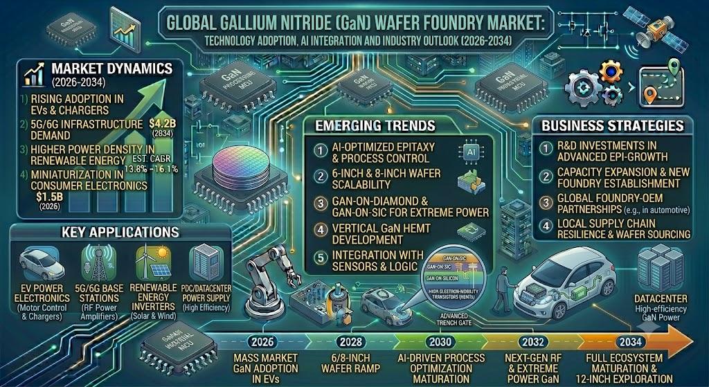
The global Gallium Nitride (GaN) Wafer Foundry Market is witnessing accelerated expansion as leading semiconductor manufacturers ramp up production of GaN-on‑Si and GaN‑on‑SiC wafers to satisfy surging demand from power‑electronics, radio‑frequency (RF) and emerging AI‑driven applications. The market’s momentum is propelled by the convergence of five‑year product road‑maps that prioritize energy‑efficient power conversion, the rollout of 5G and 6G networks, and the rapid electrification of transportation.
GaN wafers are pivotal enablers for next‑generation devices, offering higher breakdown voltage, faster switching speed and superior thermal conductivity compared with traditional silicon. These material advantages translate into lighter, more compact power modules and RF front‑ends that can operate at higher frequencies while consuming less power. Consequently, OEMs across automotive, telecommunications and aerospace are increasingly specifying GaN‑based solutions, driving foundry capacity expansions worldwide.
Download FREE Sample Report:
Gallium Nitride (GaN) Wafer Foundry Market - View in Detailed Research Report
Key Growth Catalysts
The expansion of the GaN wafer foundry market is underpinned by several intertwined forces:
- 5G/6G Infrastructure Rollout: Telecom operators are replacing silicon‑based RF power amplifiers with GaN devices to meet higher frequency bands and power‑density requirements, creating a steady demand for high‑volume wafer supply.
- Electrified Mobility: Electric‑vehicle (EV) manufacturers are integrating GaN power converters for on‑board chargers and DC‑DC converters, leveraging the technology’s high efficiency and reduced cooling needs.
- Renewable Energy Integration: Solar inverters and wind turbine converters benefit from GaN’s ability to handle higher voltages and frequencies, improving system reliability and lowering total cost of ownership.
- Governmental Support: Strategic semiconductor initiatives across APAC, Europe and North America allocate billions of dollars to develop indigenous GaN capabilities, fostering a favorable policy environment.
- Process Maturity: Advancements in Metal‑Organic Chemical Vapor Deposition (MOCVD) provide higher uniformity and yield, making large‑scale GaN wafer production economically viable.
Segment Analysis
Segment Analysis:
| Segment Category | Sub-Segments | Key Insights |
| By Type |
|
GaN-on-Si Wafer Foundry represents the dominant segment due to its cost‑effectiveness and compatibility with existing silicon fabs.
|
| By Application |
|
GaN Power Devices show significant growth potential in energy‑efficient applications.
|
| By End User |
|
Telecommunications remains the largest end‑user segment for GaN wafers.
|
| By Wafer Size |
|
6-inch Wafers are witnessing fastest adoption in the foundry market.
|
| By Production Process |
|
MOCVD (Metalorganic Chemical Vapor Deposition) dominates the production landscape.
|
Competitive Landscape
COMPETITIVE LANDSCAPE
Key Industry Players
GaN Wafer Foundry Market Dominated by Established Semiconductor Giants
The global Gallium Nitride (GaN) Wafer Foundry market features strong consolidation among top‑tier semiconductor manufacturers, with TSMC, GlobalFoundries, and UMC collectively holding significant market share. These industry leaders have aggressively expanded their GaN‑on‑Si and GaN‑on‑SiC wafer production capabilities to meet surging demand from power electronics and RF applications. TSMC in particular has emerged as the technology leader, leveraging its advanced 150 mm and 200 mm GaN wafer platforms for both commercial and defense applications.
Several specialized foundries have carved out important niches in the GaN semiconductor ecosystem. WIN Semiconductors and Episil Technology focus on high‑frequency RF applications, while X‑Fab and VIS cater to industrial power electronics. Emerging players like Chengdu Hiwafer and Sanan IC are gaining traction in China’s domestic market, supported by government semiconductor initiatives. Korea’s SK keyfoundry and Belgium’s BelGaN represent regional powerhouses expanding their GaN foundry services.
Regional Analysis
Regional Analysis: Gallium Nitride (GaN) Wafer Foundry Market
Taiwan accounts for over 60% of global GaN wafer foundry capacity, with specialized production lines for RF and power applications. The island's ecosystem includes epiwafer suppliers, testing facilities, and packaging specialists within close proximity.
Korean conglomerates are pioneering vertically integrated GaN solutions, combining wafer production with device manufacturing. This approach accelerates time‑to‑market for GaN power semiconductors in automotive and industrial applications.
Japanese companies lead in GaN substrate quality with proprietary crystal growth techniques. Research institutes collaborate closely with foundries to develop next‑generation GaN‑on‑Si and GaN‑on‑GaN wafer technologies.
Chinese foundries are rapidly scaling GaN wafer production with government backing. Domestic players focus on cost‑competitive GaN solutions for consumer electronics and renewable energy applications.
North America
North America shows strong GaN wafer foundry activity centered around specialized fabrication facilities in California and Massachusetts. The region excels in RF GaN technologies for defense and aerospace applications, with close university‑industry collaboration driving innovation. Venture‑capital funding supports numerous GaN startup foundries developing niche wafer solutions. The U.S. Department of Defense initiatives provide stability for GaN wafer production despite commercial market fluctuations.
Europe
European GaN wafer foundries focus on industrial and automotive quality standards, with Germany and France leading production. The region benefits from strong research in GaN power electronics at institutes like Fraunhofer. Collaborative programs between EU members aim to reduce reliance on Asian foundries for critical GaN components in energy infrastructure and transportation systems.
Middle East & Africa
The MEA region is developing GaN wafer capabilities through strategic partnerships with Asian and European foundries. Investments in semiconductor infrastructure in Saudi Arabia and the UAE aim to create localized GaN production for telecommunications and oil‑/gas applications. The region shows particular interest in GaN solutions for harsh‑environment operations.
South America
South America's GaN wafer market remains nascent but shows growth potential in Brazil’s electronics manufacturing sector. Local foundries are exploring partnerships for GaN power device production to serve regional automotive and renewable energy markets. Government incentives aim to attract foreign GaN technology transfer.
Emerging Opportunities
Beyond the traditional power‑electronics and RF drivers, several forward‑looking trends are poised to reshape the GaN wafer landscape:
- AI‑enabled Process Optimization: Foundries are deploying machine‑learning models to predict epitaxial growth outcomes, reducing scrap rates by up to 30% and shortening cycle times.
- Integration with Silicon‑Photonic Platforms: Hybrid GaN‑on‑Si solutions are emerging for data‑center transceivers, offering combined high‑speed optical and electronic performance.
- Automotive‑Grade Qualification: ISO 26262 and functional‑safety certifications are being pursued by leading foundries, opening doors to high‑volume automotive power stages.
- Supply‑Chain Resilience Initiatives: Multi‑sourcing strategies and on‑shore capacity expansions are being funded to mitigate geopolitical risks and raw‑material shortages.
Report Scope and Availability
The comprehensive research report delivers an in‑depth analysis of the global and regional GaN Wafer Foundry market from 2026 to 2034. It includes detailed segmentation, forecasted market sizes, competitive intelligence, technology trends, and a thorough evaluation of the key market dynamics that influence strategic decision‑making for investors, OEMs, and policy makers.
Get Full Report Here:
Gallium Nitride (GaN) Wafer Foundry Market Technology Adoption, AI Integration and Industry Outlook (2026‑2034) - View in Detailed Research Report
click here to visit more insigtfull Reports
https://semiconductorinsight.com/report/global-noncontact-level-sensors-market/embed/
https://semiconductorinsight.com/blog/tag/future-of-the-printed-circuit-board-market-growth/
About Semiconductor Insight
Semiconductor Insight is a leading provider of market intelligence and strategic consulting for the global semiconductor and high‑technology industries. Our in‑depth reports and analysis offer actionable insights to help businesses navigate complex market dynamics, identify growth opportunities, and make informed decisions. We are committed to delivering high‑quality, data‑driven research to our clients worldwide.
🌐 Website: https://semiconductorinsight.com/
📞 International: +91 8087 99 2013
🔗 LinkedIn: Follow Us