

Wafer Grinding & Thinning Market, Trends, Business Strategies 2026-2034
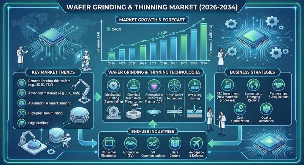
The global Wafer Grinding & Thinning Market is on a trajectory of significant expansion, driven by the relentless push for smaller, faster and more power‑efficient semiconductor devices. Industry analysts anticipate that the market will continue to deepen its footprint across advanced packaging, heterogeneous integration and next‑generation logic nodes through 2034.
Wafer grinding and thinning processes are critical to achieving the sub‑100 µm thicknesses required for high‑density interconnects, 3‑D stacking and flexible electronics. By precisely removing bulk silicon while preserving surface integrity, these technologies enable higher yields, lower material consumption and superior electrical performance, positioning them as indispensable components of modern semiconductor fabs.
Download FREE Sample Report:
Wafer Grinding & Thinning Market - View in Detailed Research Report
Semiconductor Industry Expansion: The Primary Growth Engine
The report identifies the explosive growth of the global semiconductor ecosystem as the paramount catalyst for wafer grinding and thinning demand. With semiconductor capital expenditures projected to exceed US$ 120 billion annually, the need for precision backend equipment has become a direct and substantial growth vector. The rapid adoption of advanced packaging formats such as fan‑out wafer‑level packaging (FOWLP), chip‑on‑wafer (CoW) and heterogeneous integration further intensifies the requirement for ultra‑thin wafer handling solutions.
“The concentration of leading foundries and integrated device manufacturers (IDMs) in the Asia‑Pacific region, which accounts for roughly three‑quarters of global wafer‑processing capacity, fuels the market’s dynamism,” the study notes. Ongoing investments in 5 nm and sub‑5 nm process nodes, together with the rollout of 300 mm (12‑inch) and emerging 450 mm (18‑inch) wafer platforms, are expected to amplify demand for high‑precision grinding and polishing equipment that can sustain sub‑10 µm surface‑roughness specifications.
Market Segmentation: Ultra‑Thin Wafers and Advanced Packaging Lead
The market can be broadly segmented by type, application, end‑user, technology and wafer size. While each segment contributes to overall growth, the ultra‑thin wafer and advanced packaging sub‑segments demonstrate the highest momentum due to escalating device miniaturization and the proliferation of 3‑D IC architectures.
Segment Analysis:
| Segment Category | Sub-Segments | Key Insights |
| By Type |
|
Ultra‑Thin Wafers segment demonstrates higher growth potential due to:
|
| By Application |
|
Consumer Electronics maintains leadership with critical factors including:
|
| By End User |
|
IDMs (Integrated Device Manufacturers) show significant adoption due to:
|
| By Technology |
|
Chemical Mechanical Polishing emerges as preferred technology because:
|
| By Wafer Size |
|
300 mm (12‑inch) wafers dominate the market owing to:
|
COMPETITIVE LANDSCAPE
Key Industry Players
Global Wafer Grinding & Thinning Market Leaders and Disruptors
The wafer grinding & thinning market is dominated by specialized semiconductor equipment manufacturers, with DISCO Corporation and AXUS Technology leading global market share due to their advanced precision grinding systems. These established players maintain strong R&D capabilities, particularly in ultra‑thin wafer processing below 100 µm thickness, serving major semiconductor fabs worldwide. The top five companies collectively accounted for approximately 40% of the 2025 market revenue, with Japanese and American firms showing particular strength in high‑end thinning technologies.
A growing segment of mid‑sized specialists like SIEGERT WAFER GmbH and Optim Wafer Services are gaining traction through niche capabilities in compound semiconductor processing and MEMS wafer thinning. Chinese manufacturers including Huahong Group and MACMIC are expanding rapidly, supported by domestic semiconductor industry growth and government initiatives, though still trailing in cutting‑edge thin wafer technologies below 50 µm thickness where Japanese and German firms maintain leadership.
List of Key Wafer Grinding & Thinning Companies Profiled
-
Syagrus Systems
-
Optim Wafer Services
-
SIEGERT WAFER GmbH
-
NICHIWA KOGYO CO.,LTD.
-
Integra Technologies
-
Valley Design
-
Helia Photonics
-
UniversityWafer, Inc.
-
Micross
-
Power Master Semiconductor Co., Ltd.
-
Enzan Factory Co., Ltd.
These companies are focusing on technological advancements such as the integration of IoT for predictive maintenance, automation of wafer‑handling robots, and geographic expansion into high‑growth regions like Asia‑Pacific to capitalize on emerging opportunities.
Emerging Opportunities in 5G, AI, Automotive and EV Sectors
Beyond traditional semiconductor fab needs, the report outlines several fast‑growing verticals. The rollout of 5G infrastructure and AI‑accelerated processors demands denser interconnects, which in turn require thinner, flatter wafers. Automotive electronics, especially silicon‑carbide (SiC) and gallium‑nitride (GaN) power devices, call for precise grinding to meet stringent thermal and mechanical tolerances. Moreover, the rapid expansion of electric‑vehicle battery management ICs creates a new wave of wafer‑thinning requirements for high‑voltage, high‑reliability modules.
Industry 4.0 integration is also reshaping the landscape. Smart grinding stations equipped with real‑time metrology, AI‑driven process control and remote diagnostics can reduce unplanned downtime by up to 45 % while improving overall equipment effectiveness (OEE). Equipment vendors that embed these capabilities are positioning themselves as strategic partners for fab operators seeking to accelerate time‑to‑market.
Report Scope and Availability
The market research report delivers a comprehensive analysis of the global and regional Wafer Grinding & Thinning markets from 2026‑2034. It provides detailed segmentation, market‑size forecasts, competitive intelligence, technology trends and an evaluation of key market dynamics, enabling stakeholders to make informed strategic decisions.
Get Full Report Here:
Wafer Grinding & Thinning Market, Trends, Business Strategies 2026-2034 - View in Detailed Research Report
About Semiconductor Insight
Semiconductor Insight is a leading provider of market intelligence and strategic consulting for the global semiconductor and high‑technology industries. Our in‑depth reports and analysis offer actionable insights to help businesses navigate complex market dynamics, identify growth opportunities, and make informed decisions. We are committed to delivering high‑quality, data‑driven research to our clients worldwide.
🌐 Website: https://semiconductorinsight.com/
📞 International: +91 8087 99 2013
🔗 LinkedIn: Follow Us