

DRAM Memory Stacking Chip Market Technology Adoption, AI Integration and Industry Outlook (2026-2034)
The global DRAM Memory Stacking Chip Market is witnessing robust momentum as leading memory manufacturers intensify research and development on three‑dimensional (3D) integration technologies. Driven by exponential growth in data‑center workloads, artificial‑intelligence (AI) inference engines, high‑performance computing (HPC) clusters, and emerging edge‑compute platforms, the market is rapidly evolving from niche high‑bandwidth solutions to a mainstream cornerstone of modern system‑on‑chip (SoC) architectures.
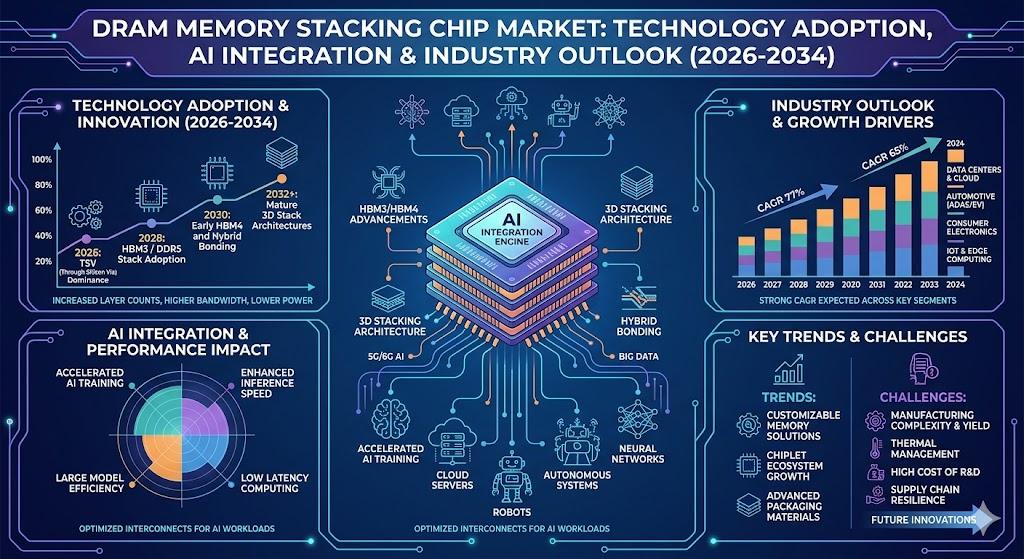
DRAM stacking chips, which combine multiple memory die in a single package using Through‑Silicon Via (TSV) or hybrid bonding, deliver unparalleled bandwidth‑to‑capacity ratios while reducing board‑level footprints and power consumption. These attributes make stacked DRAM indispensable for latency‑critical workloads such as real‑time analytics, autonomous‑vehicle perception, and immersive graphics rendering. Moreover, the ability to finely tune thermal pathways and power delivery within a stack enhances reliability across temperature‑extreme environments, reinforcing its strategic value across diverse compute ecosystems.
Download FREE Sample Report:
DRAM Memory Stacking Chip Market - View in Detailed Research Report
Semiconductor Industry Expansion: The Primary Growth Engine
The report identifies the explosive expansion of the global semiconductor industry as the foremost catalyst for stacked‑DRAM adoption. The worldwide semiconductor equipment market, already surpassing $120 billion annually, is projected to sustain double‑digit growth through 2034, propelled by relentless demand for compute power in cloud services, AI training, and 5G infrastructure. Memory‑intensive workloads now account for over 60 % of total semiconductor revenue, creating a direct and sizable demand pipeline for high‑density, high‑bandwidth memory solutions.
“The concentration of hyperscale data‑center operators and AI‑centric fab facilities in the Asia‑Pacific region, which consumes roughly three‑quarters of the global stacked‑DRAM supply, amplifies market dynamism,” the report notes. Cumulative investments in new fab capacity and advanced packaging lines are expected to exceed $500 billion by 2030, reinforcing the strategic importance of TSV‑based stacking technologies that enable sub‑nanosecond inter‑die communication and power‑efficient operation at process nodes below 20 nm.
Read Full Report: https://semiconductorinsight.com/report/dram-memory-stacking-chip-market/
Market Segmentation: Stacking Types and End‑Use Applications Dominate
The report provides a granular segmentation analysis, offering a clear view of the market structure and the principal growth segments:
Segment Analysis:
By Type
- Stacking 8 DRAM Chip
- Stacking 12 DRAM Chip
- Others
By Application
- Servers
- Mobile Devices
- Automotive Electronics
- Others
By End User
- Enterprise
- Consumer Electronics
- Automotive
By Stacking Technology
- Through‑Silicon Via (TSV)
- Package‑on‑Package (PoP)
- Hybrid Memory Cube
By Vendor Type
- IDM (Integrated Device Manufacturers)
- Fabless Companies
- Foundry Partners
Segment Analysis:
| Segment Category | Sub-Segments | Key Insights |
| By Type |
|
Stacking 8 DRAM Chip dominates the market due to its widespread adoption in mainstream applications.
|
| By Application |
|
Servers represent the fastest‑growing application segment:
|
| By End User |
|
Enterprise sector shows strongest adoption patterns:
|
| By Stacking Technology |
|
Through‑Silicon Via (TSV) technology leads in adoption:
|
| By Vendor Type |
|
IDM (Integrated Device Manufacturers) dominate the supply chain:
|
Competitive Landscape
DRAM Memory Stacking Chip Market Dominated by Memory Manufacturing Giants
The DRAM Memory Stacking Chip market is highly concentrated with three major players-SK Hynix, Samsung Electronics, and Micron Technology-collectively commanding over 80 % of global revenue share. These companies lead through advanced TSV (Through‑Silicon Via) stacking technologies and economies of scale. Samsung maintains technological leadership with its 3D‑stacked GDDR6 and HBM memory solutions, while SK Hynix specializes in high‑bandwidth memory for AI/ML applications. Micron competes through cost‑efficient production and partnerships with hyperscalers.
Emerging competitors like Nanya Technology and Winbond Electronics are gaining traction in niche segments such as low‑power DRAM for IoT devices. Chinese players (CXMT, YMTC) are accelerating R&D with government support but face technological lag in advanced nodes below 20 nm. Fabless companies like Rambus and Synopsys provide critical IP for chip designs, while OSAT firms (ASE Group, Amkor Technology) enable cost‑effective packaging solutions for stacked DRAM architectures.
List of Key DRAM Memory Stacking Chip Companies Profiled
-
Nanya Technology
-
Winbond Electronics
-
Powerchip Technology
-
ChangXin Memory Technologies (CXMT)
-
Yangtze Memory Technologies (YMTC)
-
Amkor Technology
-
Synopsys
-
Texas Instruments
-
Intel Corporation
-
Toshiba Memory
Emerging Opportunities in AI‑Driven Edge Computing and Automotive Domains
Beyond the traditional data‑center and HPC drivers, the report highlights several high‑growth verticals that are reshaping the demand landscape for stacked DRAM. In the automotive sector, next‑generation driver‑assistance systems and autonomous‑vehicle platforms require massive on‑board memory bandwidth to process sensor fusion data in real time. Stacked DRAM’s low‑latency, high‑throughput characteristics make it a natural fit for these safety‑critical applications.
Edge‑computing nodes, increasingly deployed at the network’s periphery to support 5G‑enabled services, benefit from the compact form factor and power‑efficiency of 3D‑stacked memory. The convergence of AI inference workloads with low‑power edge devices creates a compelling incentive for manufacturers to integrate 8‑ and 12‑layer DRAM stacks directly onto silicon‑photonic or heterogeneous compute substrates.
Furthermore, the emergence of chiplet‑based system‑in‑package (SiP) architectures opens new pathways for modular memory scaling. By decoupling memory capacity from logic die, chiplets enable designers to mix‑and‑match memory stacks tailored to specific bandwidth or latency requirements, accelerating time‑to‑market for bespoke AI accelerators.
Report Scope and Availability
The market research report offers a comprehensive analysis of the global and regional DRAM Memory Stacking Chip markets from 2025‑2034. It provides detailed segmentation, market size forecasts, competitive intelligence, technology trends, and an evaluation of key market dynamics. The study also examines supply‑chain resilience, geopolitical influences, and the impact of sustainability initiatives on packaging materials and manufacturing processes.
Get Full Report Here:
DRAM Memory Stacking Chip Market Technology Adoption, AI Integration and Industry Outlook (2026-2034) - View in Detailed Research Report
About Semiconductor Insight
Semiconductor Insight is a leading provider of market intelligence and strategic consulting for the global semiconductor and high‑technology industries. Our in‑depth reports and analysis offer actionable insights to help businesses navigate complex market dynamics, identify growth opportunities, and make informed decisions. We are committed to delivering high‑quality, data‑driven research to our clients worldwide.
🌐 Website: https://semiconductorinsight.com/
📞 International: +91 8087 99 2013
🔗 LinkedIn: Follow Us