

Polysilicon Wafer Market, Emerging Trends, Technological Advancements, and Business Strategies 2025-2032
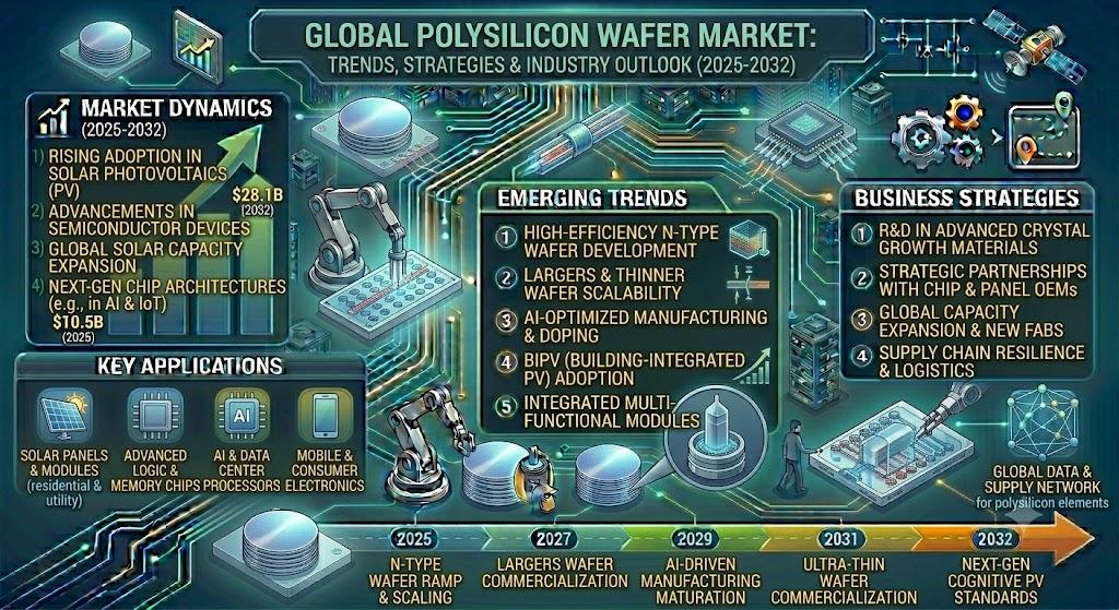
The global Polysilicon Wafer Market is experiencing a wave of demand driven by the rapid expansion of semiconductor manufacturing, the ongoing transition to renewable energy, and the acceleration of advanced photovoltaic technologies. As the foundation for both high‑performance logic chips and next‑generation solar cells, polysilicon wafers have become a strategic commodity in the high‑technology supply chain, attracting significant capital investment and policy support worldwide.
Polysilicon wafers, fabricated from ultra‑high‑purity silicon, are essential substrates for a wide spectrum of electronic and energy applications. In the semiconductor arena they support sub‑10 nm logic nodes, high‑density memory, and emerging three‑dimensional integration schemes, while in the photovoltaic sector they enable the production of high‑efficiency N‑type cells that surpass 23 % conversion rates. Their versatility, combined with ongoing cost‑reduction innovations such as advanced crystal pulling and wafer‑splitting techniques, positions polysilicon wafers as a linchpin for both digital and green economies.
Download FREE Sample Report:
Polysilicon Wafer Market - View in Detailed Research Report
Semiconductor Industry Expansion: The Primary Growth Engine
The report highlights the explosive growth of the global semiconductor sector as the paramount catalyst for polysilicon wafer demand. With semiconductor foundries scaling to 300 mm wafer platforms for advanced logic and memory production, the need for defect‑free, high‑purity wafers is intensifying. Investment announcements from leading chipmakers indicate a cumulative spend exceeding $500 billion on new fab capacity through 2030, a trajectory that directly fuels wafer consumption. Moreover, the shift toward heterogeneous integration and advanced packaging amplifies wafer throughput requirements across multiple technology nodes.
“The concentration of semiconductor fabs in the Asia‑Pacific region, which now accounts for roughly 78 % of global wafer processing capacity, is a decisive factor in shaping market dynamics,” the study notes. Government‑backed initiatives, such as the United States CHIPS Act ($52 billion) and the European Chips Act (€43 billion), are poised to diversify the geographic footprint of wafer demand, yet the existing production ecosystem remains heavily weighted toward established Asian manufacturers.
Read Full Report: https://semiconductorinsight.com/report/polysilicon-wafer-market/
Market Segmentation: Type, Application, Diameter, and End‑User Industry
The report provides a detailed segmentation analysis, offering a clear view of the market structure and key growth segments:
Segment Analysis:
By Type
N-Type Segment Dominates Due to Higher Efficiency in Solar Cells and Semiconductor Applications
The market is segmented based on type into:
-
P Type
-
Widely used in power devices due to stable performance
-
-
N Type
By Application
Semiconductor Segment Leads the Market Owing to Increasing Electronic Device Production
The market is segmented based on application into:
-
Semiconductor
-
Photovoltaic
-
Other
By Diameter
300 mm Wafers Dominate Production Due to Higher Cost Efficiency in Semiconductor Fabrication
The market is segmented based on diameter into:
-
150 mm
-
200 mm
-
300 mm
-
Others
By End‑User Industry
Consumer Electronics Sector Shows Strong Growth Due to Expanding Smart Device Market
The market is segmented based on end‑user industry into:
-
Consumer Electronics
-
Automotive
-
Industrial
-
Energy
-
Others
Download Sample Report: https://semiconductorinsight.com/download-sample-report/?product_id=117516
COMPETITIVE LANDSCAPE
Key Industry Players
Innovation and Capacity Expansion Drive Competition in the Polysilicon Wafer Market
The global polysilicon wafer market exhibits a semi‑consolidated competitive landscape, dominated by established manufacturers while witnessing emerging players making strategic moves. China‑based Zhonghuan Semiconductor and Xinjiang Daqo New Energy currently lead the market, collectively accounting for over 30 % of global production capacity as of 2024. Their dominance stems from vertical integration strategies and government‑backed expansion projects in the photovoltaic sector.
Meanwhile, GCL TECH has emerged as a formidable competitor through technological advancements in high‑purity polysilicon production, reducing manufacturing costs by approximately 18 % since 2022. The company's focus on N‑type wafer technology has positioned it strongly in the premium solar wafer segment.
Established semiconductor wafer specialists like WaferPro and TRINITY maintain strong positions in the 300 mm wafer segment, catering to advanced logic and memory chip manufacturers. These companies are investing heavily in defect reduction technologies, achieving zero dislocation rates in their prime‑grade wafers.
The competitive intensity is further heightened by regional players like JYT Corporation and Danen Technology pursuing aggressive capacity expansions. JYT Corporation recently announced a $2.1 billion investment to establish a new production facility in Vietnam, aiming to capitalize on Southeast Asia's growing semiconductor ecosystem.
These companies are focusing on technological advancements such as AI‑driven defect inspection, IoT‑enabled production monitoring, and low‑carbon polysilicon processes. Geographic expansion into high‑growth regions-including Southeast Asia, Eastern Europe, and the United States-is a recurring strategic theme, aimed at mitigating supply‑chain risks and capturing emerging demand pockets.
Emerging Opportunities in EV, Renewable Energy, and Industry 4.0
The rapid scaling of electric‑vehicle (EV) battery manufacturing and the broader renewable‑energy transition are creating new demand vectors for high‑efficiency N‑type wafers. Modern EV battery packs require power‑electronics modules that operate at higher voltages and lower losses, driving semiconductor vendors to adopt advanced node technologies that rely on pristine polysilicon substrates. Simultaneously, large‑scale solar farms are migrating from P‑type to N‑type cell architectures to achieve higher energy yields, directly boosting wafer consumption.
Industry 4.0 initiatives are reshaping wafer production lines through the integration of smart sensors, real‑time analytics, and predictive maintenance platforms. According to the report, smart‑factory implementations can cut unplanned equipment downtime by up to 45 % and improve overall equipment effectiveness (OEE) by 12‑15 %, delivering tangible cost benefits for wafer manufacturers.
Report Scope and Availability
The market research report offers a comprehensive analysis of the global and regional polysilicon wafer markets from 2025 – 2032. It provides detailed segmentation, market size forecasts, competitive intelligence, technology trends, and an evaluation of key market dynamics. The study also examines policy influences, investment pipelines, and supply‑chain considerations that shape the competitive environment.
Get Full Report Here:
Polysilicon Wafer Market, Emerging Trends, Technological Advancements, and Business Strategies 2025-2032 - View in Detailed Research Report
click here to visit more insigtfull Reports
https://semiconductorinsight.com/report/global-noncontact-level-sensors-market/embed/
https://semiconductorinsight.com/blog/tag/future-of-the-printed-circuit-board-market-growth/
About Semiconductor Insight
Semiconductor Insight is a leading provider of market intelligence and strategic consulting for the global semiconductor and high‑technology industries. Our in‑depth reports and analysis offer actionable insights to help businesses navigate complex market dynamics, identify growth opportunities, and make informed decisions. We are committed to delivering high‑quality, data‑driven research to our clients worldwide.
🌐 Website: https://semiconductorinsight.com/
📞 International: +91 8087 99 2013
🔗 LinkedIn: Follow Us