

Die-to-Wafer (D2W) Collective Bonding Market, Trends, Business Strategies 2026-2034
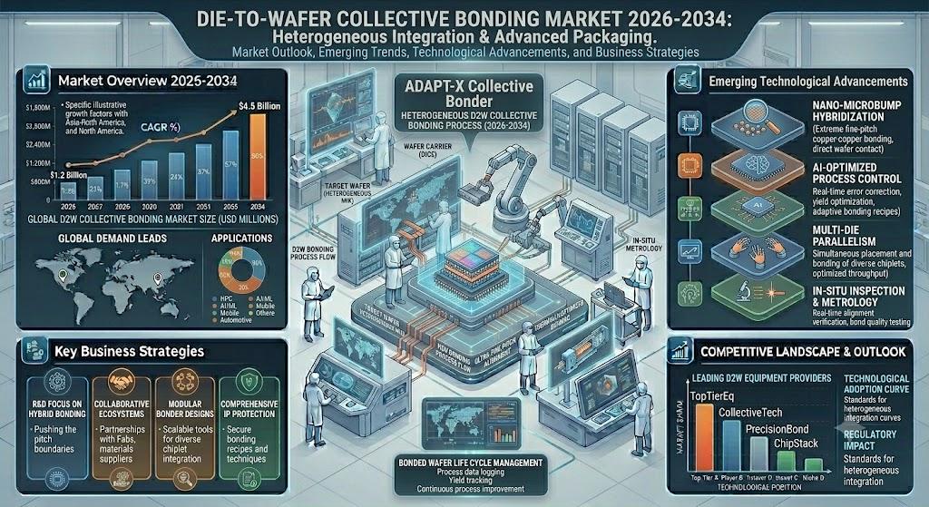
The global Die-to-Wafer (D2W) Collective Bonding Market is witnessing accelerating interest as semiconductor manufacturers pursue higher levels of three‑dimensional integration and heterogeneous system‑in‑package (SiP) architectures. The surge in artificial‑intelligence (AI) workloads, high‑performance computing (HPC) demands, and the migration to advanced node technologies are compelling equipment vendors to adopt D2W collective bonding as a core enabler for sub‑micron interconnects and ultra‑dense stacking.
D2W collective bonding delivers a combination of superior thermal management, enhanced electrical performance, and significantly higher yield compared with traditional point‑bonding approaches. By bonding an entire wafer to another wafer in a single step, manufacturers can reduce cycle time, improve alignment precision, and lower overall production cost-critical factors for maintaining competitive advantage in a market where time‑to‑volume is increasingly decisive.
Download FREE Sample Report:
Die-to-Wafer (D2W) Collective Bonding Market - View in Detailed Research Report
Semiconductor Industry Expansion: The Primary Growth Engine
The report identifies the relentless expansion of the global semiconductor ecosystem as the paramount catalyst for D2W collective bonding adoption. Foundries are scaling to produce multi‑chip modules (MCMs) that integrate logic, memory, and specialty dies within a single stack. The need to sustain Moore‑law‑type performance gains while managing thermal budgets drives a shift toward bonding technologies that can reliably support high‑density interconnects without compromising device reliability.
Strategic investments exceeding hundreds of billions of dollars in new fab capacity, advanced packaging lines, and research collaborations are reshaping the market landscape. In particular, the convergence of silicon photonics, RF front‑ends, and power‑electronics within heterogeneous packages places D2W collective bonding at the forefront of next‑generation system design.
COMPETITIVE LANDSCAPE
Key Industry Players
Global D2W Collective Bonding Market Analysis and Technology Trends
The competitive landscape for the Die-to-Wafer (D2W) collective bonding market is defined by the dominance of established semiconductor equipment manufacturers focused on high-density integration. These key industry players are aggressively investing in research to innovate thermocompression, hybrid, and eutectic bonding technologies essential for 3D integrated circuits. As demand for AI and high‑performance computing solutions rises, the market structure is consolidating, with leaders prioritizing reliability and yield improvements in their collective bonding processes to cater to advanced system‑in‑package applications.
A significant aspect of this landscape involves strategic collaborations between equipment vendors and research institutes to develop scalable production processes. Recent initiatives, such as the pivotal partnership in March 2024 between Besi and Imec, underscore the industry's move toward standardized D2W solutions for mass fabrication. Additionally, specialized niche players contribute by providing unique materials and laser bonding technologies, ensuring a diverse and resilient ecosystem that addresses complex thermal management and electrical performance requirements.
List of Key D2W Collective Bonding Companies Profiled
-
ASM Pacific Technology
-
EV Group
-
Applied Materials
-
Kulicke & Soffa
-
TSV Technology
-
Microconnects
-
Coherent
-
SUSS MicroTec
-
FormFactor
-
J-Devices
-
Hoya Corporation
-
NSG Group
-
JPT Corp.
D2W Collective Bonding Market Segment Analysis:
| Segment Category | Sub-Segments | Key Insights |
| By Type |
|
Hybrid Bonding dominates the landscape due to its superior capability for sub‑micron interconnects, which is essential for next‑generation semiconductor requirements. Thermocompression bonding remains a robust choice for its high reliability in high‑temperature environments and well‑established process maturity. |
| By Application |
|
High‑Performance Computing & AI are primary drivers, necessitating advanced thermal management and signal integrity that D2W technology uniquely provides. The trend towards System‑in‑package (SiP) architectures is accelerating as the industry seeks to merge logic and memory technologies without sacrificing physical density. |
| By End User |
|
Semiconductor Foundries are the leading segment, heavily investing in packaging infrastructure to maintain technological leadership in advanced manufacturing. OEMs are pivoting towards integrated solutions to reduce system complexity and cost while meeting escalating performance expectations in the consumer market. |
| By Integration Technology |
|
Heterogeneous Integration is critical for combining distinct technologies-such as logic, memory, and sensors-onto a single die, which drastically reduces power consumption and latency. This approach fundamentally redefines system architecture by allowing diverse materials to coexist within a unified package structure. |
| By Process Capability |
|
Scalable Mass Production remains a key focus area as the industry transitions from laboratory prototyping. Successful adoption requires robust yield management and precise alignment technologies to ensure consistency across large wafer volumes, reducing overall manufacturing costs. |
Regional Analysis: Die-to-Wafer (D2W) Collective Bonding Market, Trends, Business Strategies 2026-2034
The expansion of manufacturing capabilities in the United States and Canada is reshaping the market landscape. By leveraging the technical advantages of D2W collective bonding, local fabs are reducing thermal stress during wafer processing. The emphasis on next‑generation packaging solutions pushes suppliers to optimize production lines for high yield and reliability.
D2W technology is critical for the automotive sector’s transition toward electric and autonomous vehicles. The market adapts to rigorous thermal and electrical specifications required by next‑gen power modules, supporting higher performance and durability in critical applications.
Regional players are implementing sophisticated logistics to support the market. Collaborative efforts drive efficiency, ensuring that collective bonding materials reach fabrication facilities with minimal delay. Strong industry standards established in North America provide a benchmark for quality and precision, reinforcing market stability.
Research institutions are closely aligned with private industry to advance D2W capabilities. This synergy fosters development of novel bonding chemistries that withstand extreme operating conditions, and the drive toward hybrid integration signals a promising future for the region.
Europe
Europe is establishing a strong foothold in the Die-to-Wafer Collective Bonding Market, primarily fueled by the automotive industry’s demand for efficient power management and thermal dissipation. With strict environmental regulations accelerating the shift toward electrified mobility, European manufacturers are integrating advanced collective bonding. The market in Europe relies heavily on synergy between research labs and established automotive giants. While capital investment in new fabs is slower than in Asia‑Pacific, the maturity of the existing supply chain ensures a steady demand for high‑quality bonding solutions. Europe’s commitment to industrial sovereignty and energy‑efficiency standards continues to bolster market resilience.
Asia‑Pacific
Asia‑Pacific represents the largest production hub for the Die-to-Wafer Collective Bonding Market, characterized by high‑volume fabrication and rapid technological iteration. The region’s dominance is bolstered by foundries that specialize in scaling 3D chip stacking. As global demand for miniaturized electronics grows, the market sees rapid adoption of volume‑production techniques. Cost advantages, supply‑chain agility, and strong governmental support keep Asia‑Pacific at the centre of worldwide output, driving continuous innovation in bonding materials and equipment.
South America
South America is witnessing a nascent yet growing interest in the market, driven by modernization of telecommunications and energy infrastructure. Although volumes remain modest, the strategic importance of efficient semiconductor packaging is becoming increasingly apparent. Nations are aligning market development with broader economic goals, importing advanced packaging technologies to transition from assembly‑only operations toward localized production, and focusing on solutions that support smart‑grid and urban‑planning applications.
Middle East & Africa
The Middle East and Africa are emerging markets for D2W collective bonding, heavily influenced by vision‑led economic diversification plans such as NEOM and Vision 2030. Demand is less mature but evolving quickly as countries invest in smart‑city technologies and advanced digital infrastructure. The market is characterized by a need for durable electronic components capable of withstanding harsh environmental conditions. While supply chains are still developing, strategic alliances with global technology providers are expected to accelerate adoption of collective bonding technologies across the region.
Get Full Report Here:
Die-to-Wafer (D2W) Collective Bonding Market, Trends, Business Strategies 2026-2034 - View in Detailed Research Report
About Semiconductor Insight
Semiconductor Insight is a leading provider of market intelligence and strategic consulting for the global semiconductor and high-technology industries. Our in‑depth reports and analysis offer actionable insights to help businesses navigate complex market dynamics, identify growth opportunities, and make informed decisions. We are committed to delivering high‑quality, data‑driven research to our clients worldwide.
🌐 Website: https://semiconductorinsight.com/
📞 International: +91 8087 99 2013
🔗 LinkedIn: Follow Us